
Comprehensive analysis of the PCB topology in Altair PollEx for Altium Designer.
Part 1. Checking the topology before production.
The introduction of modeling into the PCB development process allows design engineers to identify potential problems in the manufacture and installation of printed circuit boards at the early stages of design. Verification of the PCB topology is a necessary step to reduce production, financial and time costs. The integrated approach includes checking both the electrical characteristics of the printed circuit board (DFE, DFE+, LDFE) and the parameters for the manufacture and installation of the printed circuit board (DFM, DFA). The article discusses the possibilities of Altair PollEx, a software solution from Altair Engineering, designed for the analysis, verification and verification of printed circuit boards at any design stage.
Modern software tools provide powerful tools to quickly and accurately detect widespread PCB defects that would otherwise require careful manual analysis, laboratory testing, or field testing. Altair PollEx is a software solution that significantly accelerates the development of electronic devices through comprehensive modeling and verification of the topology of the printed circuit board (Fig. 1).
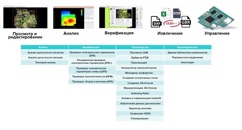
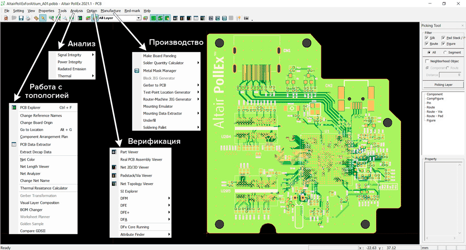
Altair PollEx includes tools for signal integrity analysis (SI) and power supply (PI), thermal analysis (Thermal), as well as conducting more than 1,500 topology checks for manufacturability (DFM), assembly and installation (DFA), compliance with electrical characteristics (DFE) from a single interface (Fig. 2).
Signal integrity analysis tools allow you to analyze and optimize signal transmission lines, perform eye diagram analysis, crosstalk, DDR memory. These tools provide an opportunity to perform analysis in the time and frequency domain. Power integrity analysis makes it possible to analyze noise (crosstalk) while switching signals at the same time, as well as perform an analysis of DC voltage drop, an analysis of AC power distribution, an analysis of AC power supply using decoupling capacitors.
Thermal analysis of the printed circuit board is carried out using the finite element method. The grid is built automatically, the temperature is calculated on the upper and lower sides of the component body, taking into account the transition temperature. The user can set boundary conditions and add radiators to improve the characteristics of the printed circuit board.
Verification of the PCB topology for compliance with electrical characteristics includes more than 400 checks. The rules are grouped into categories: rules for high-speed signals, differential pairs, circuits, power supply, components, and board topology. The user can find violations related to the location of the transition holes, shielding, reverse current paths, length and width of differential pairs, etc. To increase efficiency, you can configure the rules, export them to a separate file and use them later in topology verification.
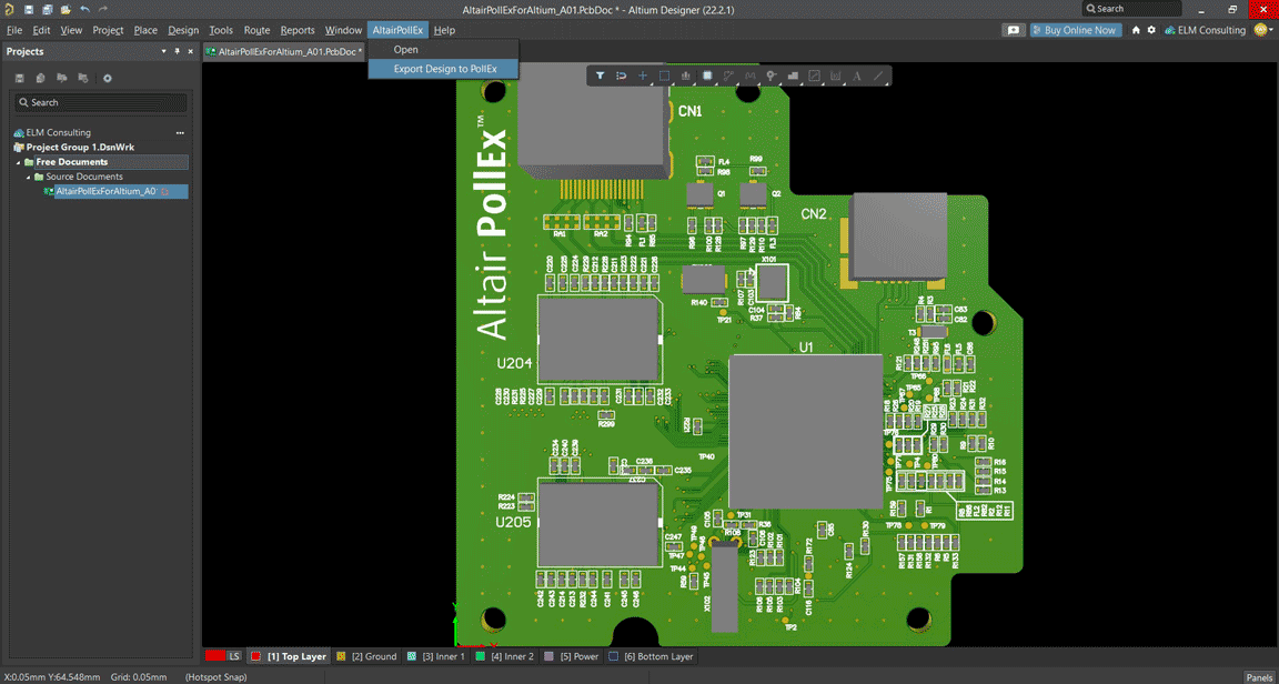
A limited version of Altair PollEx for Altium is available to Altium Designer users for free (more details), which allows for basic signal integrity analysis, thermal analysis, electrical verification and PCB manufacturability analysis. To install Altair PollEx, go to the Extensions and Updates tab and select Altair PollEx to install. After installation, a separate Altair PollEx tab will appear in the Altium Designer menu (Fig. 3). The close integration of Altium Designer and Altair PollEx allows the developer to export designs and conduct comprehensive analysis and verification of the PCB topology. Detected errors are highlighted in Altium Designer and can be corrected immediately.
Thermal analysis of the printed circuit board is carried out using the finite element method. The grid is built automatically, the temperature is calculated on the upper and lower sides of the component body, taking into account the transition temperature. The user can set boundary conditions and add radiators to improve the characteristics of the printed circuit board.
Verification of the PCB topology for compliance with electrical characteristics includes more than 400 checks. The rules are grouped into categories: rules for high-speed signals, differential pairs, circuits, power supply, components, and board topology. The user can find violations related to the location of the transition holes, shielding, reverse current paths, length and width of differential pairs, etc. To increase efficiency, you can configure the rules, export them to a separate file and use them later in topology verification.
A limited version of Altair PollEx for Altium is available to Altium Designer users for free (more details), which allows for basic signal integrity analysis, thermal analysis, electrical verification and PCB manufacturability analysis. To install Altair PollEx, go to the Extensions and Updates tab and select Altair PollEx to install. After installation, a separate Altair PollEx tab will appear in the Altium Designer menu (Fig. 3). The close integration of Altium Designer and Altair PollEx allows the developer to export designs and conduct comprehensive analysis and verification of the PCB topology. Detected errors are highlighted in Altium Designer and can be corrected immediately.
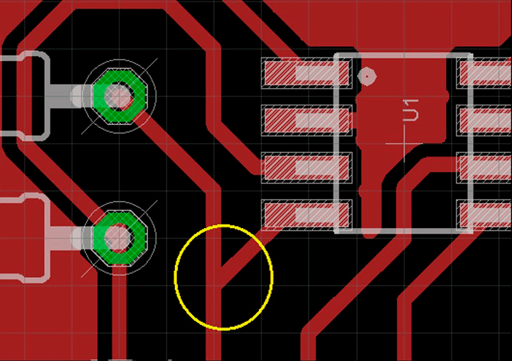
Let's consider Altair PollEx verification tools for analyzing the manufacturability of the PCB topology, which allow us to detect common manufacturing errors. During the production process, such a defect may occur as acid traps – places of scratches on the printed circuit board, which are most often formed in sharp corners between the conductors (Fig. 4). Conductors connected at an angle of less than 90 ° create traps during the production process where residual acid is collected, especially before washing the board. This can cause corrosion or circuit breakage, which leads to failure.
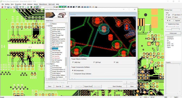
It should be noted that conductors connected to transition or through holes without teardrop connections can also lead to the appearance of acid traps. With Altair PollEx, an engineer can check the trace for sharp corners. This check detects the conductors connected to the pads at an angle of 90°, which will correct the trace, which can cause problems with etching. As a result of this check, chains whose trace angle differs from 45 or 90° will also be marked. Using the Teardrops check allows you to identify contact pads without teardrop-shaped connections, in particular for components in a DIP type housing, where there is a possibility of a hole breakdown (Fig. 5).
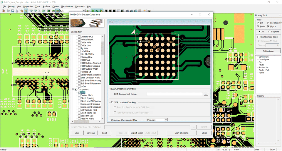
Chips in BGA type enclosures are the most commonly used component in complex high-speed high-density circuit boards. A number of factors must be considered to ensure reliable operation of BGA chips. Fixing some of the possible problems after the PCB is manufactured may entail additional costs in terms of time and resources. Most of the problems when using BGA chips are related to the pads for the "array of ball pins" located on the back of the chip. The correct size of the gaps around each contact pad ensures the correct installation of BGA chips. Using Altair PollEx, the developer can check the gap between the contact pads of the chip and the transition holes (Fig. 6). When tracing a BGA chip, the transition holes between the contact pads should ideally be located in the center of the four contact pads of the BGA case. Otherwise, the solder formed on the pads can penetrate into the transition holes, since the area of the solder mask is larger than the area of the metallized contact pad.
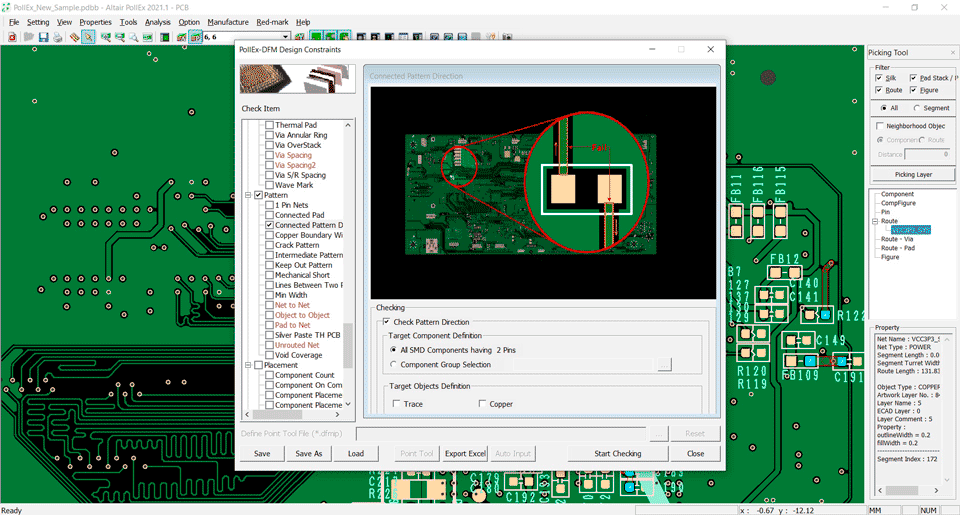
During the manufacturing process, the Tombstone effect may also occur due to improper wetting of the contact pad with solder or the withdrawal of the component. When melting the solder paste, the uneven tension force at the ends of the terminals of the component causes the component to lift on one side. With the Altair PollEx, the engineer can control the width ratio of the connected conductors to the contact pad using the Connected Pattern Direction check (Fig. 7). Due to the mismatch of the heat transfer of the two contact pads, one of them needs to be heated more strongly to ensure the correct connection. Therefore, the temperature difference will create an imbalance in the tension force when wetting with solder, which will lead to the effect of a "tombstone". To prevent the problem, it is necessary to make sure that the ratio of the width of the connected conductor and the contact pad is within acceptable limits.
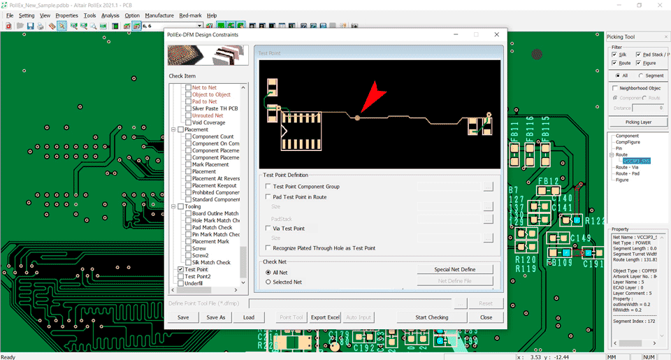
After manufacturing, the board is usually tested to make sure that there are no short circuits and breaks in the circuits. After the components are installed, the board is often retested to check the integrity of the signals and the operability of the board. For testing on the board, as a rule, so-called testpoints are provided, at which, with the help of test equipment, it is possible to take readings and perform the necessary tests. Control points are usually included in the PCB topology to test critical circuits and components related to power supply or located in hard-to-reach places, but some of them can be skipped when designing a board. Altair PollEx checks the presence of control points for the specified components and circuits (Fig. 8).
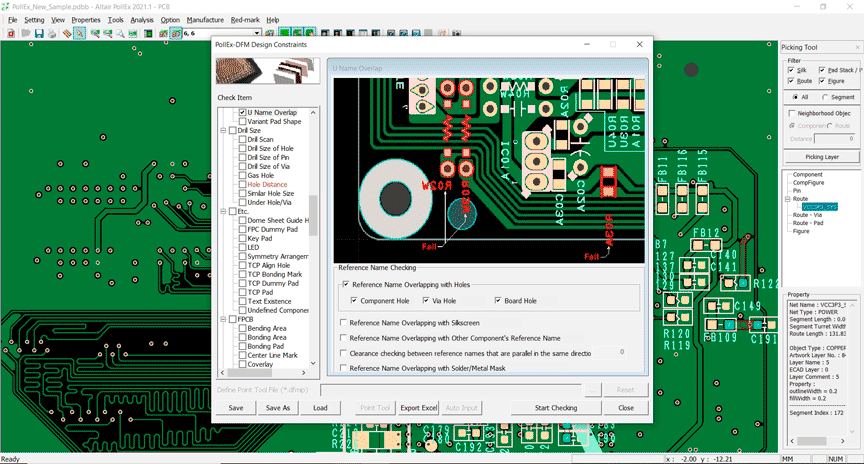
An important role in the production and installation of a printed circuit board is played by a silkscreen layer (marking layer), which is designed to facilitate the installation of components and the placement of additional reference information. The silkscreen layer contains the following information: the contours of the components, indicating the zones in which they should be installed; the indicator of the first output (for complex multi-output chips, the indicator of the first output helps to correctly place the component on the printed circuit board); positional designations (they should not be placed under the component, on top of the contact pads and transition holes, so as not to complicate the soldering process). It is important to make sure that the information located on the silkscreen layer is presented accurately in order to avoid any inconsistencies in the topology.
When using Altair Pollex, the developer can perform a Reference Name Checking, which controls the positional designations of components and the presence of the first output indicator for complex multi-output components (Fig. 9). Using the Check for reference names overlapping with other objects (components, pads and holes), the user can make sure that there are no positional intersections in the topology.x designations with other objects (components, pads, holes). It is necessary to avoid placing the positional designation on certain objects on the board in order to prevent a number of problems: silkscreen printing in holes and silkscreen printing on the conductor can create problems of signal integrity and power supply, and silkscreen printing on soldered surfaces can worsen the reliability of soldered connections.
When using Altair Pollex, the developer can perform a Reference Name Checking, which controls the positional designations of components and the presence of the first output indicator for complex multi-output components (Fig. 9). Using the Check for reference names overlapping with other objects (components, pads and holes), the user can make sure that there are no positional intersections in the topology.x designations with other objects (components, pads, holes). It is necessary to avoid placing the positional designation on certain objects on the board in order to prevent a number of problems: silkscreen printing in holes and silkscreen printing on the conductor can create problems of signal integrity and power supply, and silkscreen printing on soldered surfaces can worsen the reliability of soldered connections.
The effective transmission of the results of the verification of the PCB topology is as important as the verification itself. PollEx DFx has an export function that allows you to transfer information about the checks performed in Excel format.
In addition to PCB developers, PollEx provides an efficient work environment for SMT process technologists who can quickly obtain data for stenciling, assembly, installation and testing of printed circuit boards. Let's look at several PollEx tools that increase the efficiency of process engineers.
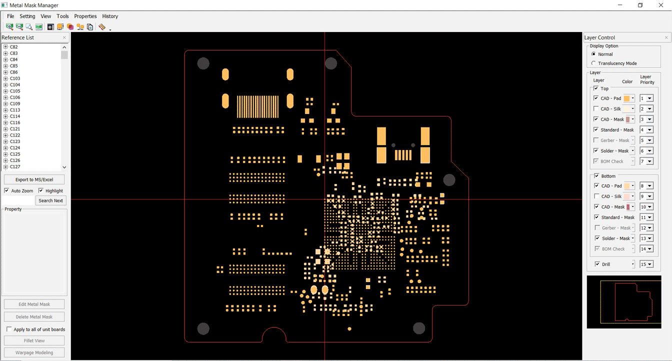
Stencil manager. After manufacturing the printed circuit board using a stencil, a layer of solder paste is applied to it for soldering surface-mounted components. After the paste is applied, the board is placed in a component installation machine. At this time, the flux contained in the solder paste holds all the parts in place until the entire component installation process is completed. Altair PollEx contains a database of standard stencils, manages the history of stencil changes and controls the differences between the topology of the printed circuit board and standard stencils from the database (Fig. 10). The user can manage multiple stencil databases or change the PCB stencil according to unified standards.
In addition to PCB developers, PollEx provides an efficient work environment for SMT process technologists who can quickly obtain data for stenciling, assembly, installation and testing of printed circuit boards. Let's look at several PollEx tools that increase the efficiency of process engineers.
Stencil manager. After manufacturing the printed circuit board using a stencil, a layer of solder paste is applied to it for soldering surface-mounted components. After the paste is applied, the board is placed in a component installation machine. At this time, the flux contained in the solder paste holds all the parts in place until the entire component installation process is completed. Altair PollEx contains a database of standard stencils, manages the history of stencil changes and controls the differences between the topology of the printed circuit board and standard stencils from the database (Fig. 10). The user can manage multiple stencil databases or change the PCB stencil according to unified standards.
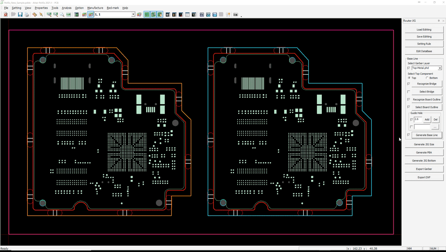
Creating JIG blocks. The creation of JIG blocks in Altair PollEx is used to test the manufacturability of printed circuit boards in terms of screen printing equipment (Fig. 11). The stable position of the printed circuit board ensures uniform solder application during surface mounting. When changing the shape of the printed circuit board, it is also necessary to adjust the JIG blocks. Rapid creation of a design drawing with JIG blocks is possible using the design data of the printed circuit board, Gerber files or multiplication of the printed circuit board (combining several drawings of the printed circuit board on one blank to reduce production costs).
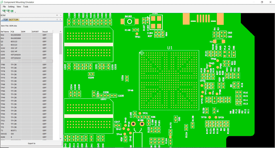
The installation emulator. Altair PollEx includes a set of tools for installation verification based on libraries of 3D components created using UPE (PollEx Unified Part Library Editor). The developer can check the correctness of the component location, as well as analyze the coordinates and angles of the component placement (Fig. 12). The results can be exported to Microsoft Excel.
Altair Engineering's software solutions provide an opportunity for engineers to work together on all aspects of PCB development, including complex and interdisciplinary modeling. Using Altair PollEx allows you to optimize the design process and reduce time to market, while ensuring high performance, reliability and compliance with standards.