Electronics
Electronics are a part of our lives – both professionally and personally – with the latest gadgets delivering an immediate gateway to the world. Innovation, time to market and lower cost are the keys to electronics success, and the pressures to quickly deliver innovative products at lower cost is intense. Altair’s simulation-driven design delivers a smarter approach to electronics product development.
Shorten Time to Market
Manufacturers dedicate large amounts of time and expense to physical prototyping in order to validate product performance. Simulation can dramatically speed up time-to-market by enabling the testing of multiple design concepts and variables virtually. Multiple variants can be efficiently tested at a massive scale without physical testing and repeated redesign iterations. Replacing even one prototyping cycle with simulation could mean getting products to the market months faster than the competition.

Build Smarter Products
New product lines, recurring revenue streams, more efficient operations, higher quality and faster time to market are all within reach with Internet of Things (IoT) from Altair. We have the knowledge and technology to help you realize your smart product development vision from beginning to end – from ideation to optimization to launch and operation.
Enhance Product Design
Electronic devices of all kinds must be designed to withstand the structural and operational requirements associated with normal use, drop and misuse, all while balancing weight and cost considerations. Altair solutions enable simulation of structural, thermal and fluid properties, vibration, electromagnetics and manufacturing constraints in an integrated multiphysics environment.
Delivering Functionality
PCB Design: Altair® PollEx™ is the most comprehensive and integrated set of PCB design viewing, analysis and verification tools for electrical, electronics and manufacturing engineers. PollEx transfers data flawlessly between the industry’s most popular ECAD and simulation tools and enables many of the world’s major electronics corporations to quickly visualize and review PCB designs. Its checking tools detect issues early to avoid product failures, and simplify manufacturing and assembly.
Develop Embedded Systems: Altair® Embed® is a proven tool for developing embedded systems that automatically generates efficient code from block diagram models. Once you have a working simulation based developed with a system diagram, code is automatically generated specifically for your target microcontroller hardware. Testing a design using hardware-in-the-loop (HIL) is straightforward and the robust and reliable process requires no editing of code.
Develop Embedded Systems: Altair® Embed® is a proven tool for developing embedded systems that automatically generates efficient code from block diagram models. Once you have a working simulation based developed with a system diagram, code is automatically generated specifically for your target microcontroller hardware. Testing a design using hardware-in-the-loop (HIL) is straightforward and the robust and reliable process requires no editing of code.

High-throughput Computing for Semiconductor Design
Trusted for semiconductor design and electronic design automation (EDA), Altair’s optimization solutions for high-throughput computing environments help you arrive at the perfect design faster. Take advantage of the industry’s fastest enterprise job scheduler with scalable, event-driven architecture for the highest throughput and sub-millisecond latency — and go global with seamless scheduling across geographies and business units. Get software license monitoring and real-time insight into license availability, usage, job status, and more, plus the detailed I/O profiling and telemetry you need to ensure top compute, network, and storage performance. Our unique flow tracing platform lets you map and execute even the most complex design flows.
Looking for solutions for PCB development?
Delighting Customers
From Conceptual Design to Reality: Altair’s industrial design services can help customers with everything from user research to branding to design and prototyping. Altair® Inspire™ Studio software enhances creativity. Users can combine different modeling techniques to effortlessly create and explore even the most challenging designs.
Antenna Design and Placement: Altair® Feko®is widely used for the design of radio and TV, wireless, cellular, communication, remote keyless entry, tire pressure monitoring, satellite positioning, radars, RFID and other antennas. Feko’s Method of Moments (MoM) solver is used for antenna design. Model decomposition is possible with accelerated full-wave methods like Multi-level Fast Multipole Method (MLFMM), or asymptotic methods like Physical Optics (PO), Ray Launching Geometrical Optics (RL-GO) or Uniform Theory of Diffraction (UTD).
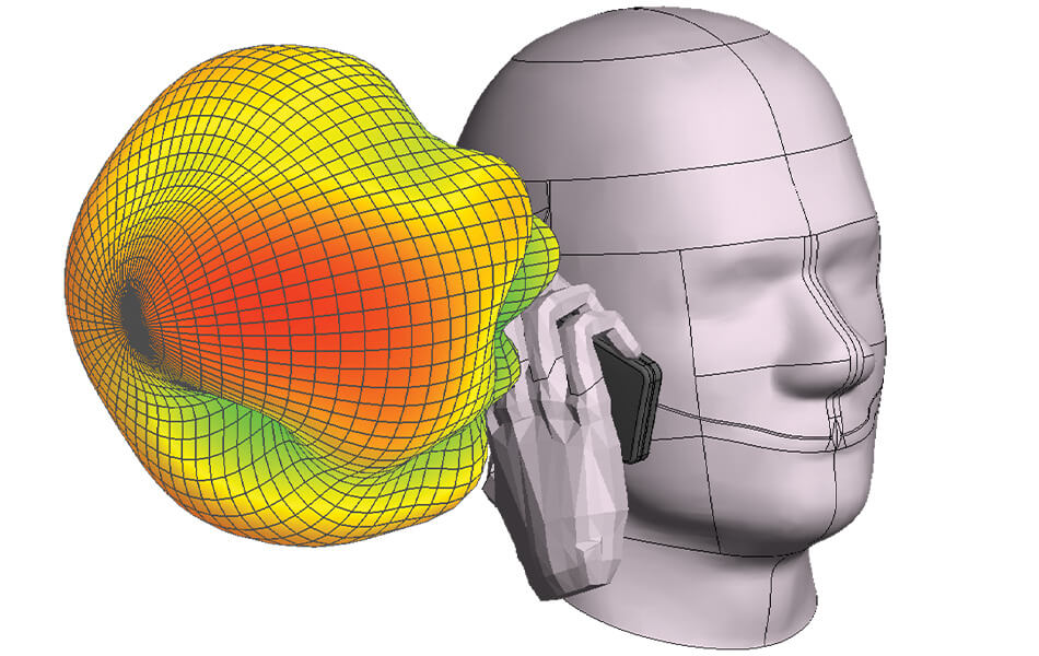
Device Compatibility: Electromagnetic compatibility (EMC) and electromagnetic interference (EMI) have become key topics with the proliferation of connected devices, both for component integration and satisfying EMC regulatory requirements. Feko can simulate both the radiation and irradiation of cables, antennas, and devices to inform the design of effective shielding. Feko also provides insight into the interactions of electromagnetic fields close to the body, ensuring safety while enough signal is radiated.
Antenna Design and Placement: Altair® Feko®is widely used for the design of radio and TV, wireless, cellular, communication, remote keyless entry, tire pressure monitoring, satellite positioning, radars, RFID and other antennas. Feko’s Method of Moments (MoM) solver is used for antenna design. Model decomposition is possible with accelerated full-wave methods like Multi-level Fast Multipole Method (MLFMM), or asymptotic methods like Physical Optics (PO), Ray Launching Geometrical Optics (RL-GO) or Uniform Theory of Diffraction (UTD).
Device Compatibility: Electromagnetic compatibility (EMC) and electromagnetic interference (EMI) have become key topics with the proliferation of connected devices, both for component integration and satisfying EMC regulatory requirements. Feko can simulate both the radiation and irradiation of cables, antennas, and devices to inform the design of effective shielding. Feko also provides insight into the interactions of electromagnetic fields close to the body, ensuring safety while enough signal is radiated.